
Popular Nanofabrication - Introduction
I wrote a thesis as part of my masters degree in materials science and I was kind of surprised to see that people actually read it. The publisher sends me a report every month with the number of views and it’s about 10 each time. Not bad!
I really tried to write it in a way that could be read by someone with a background in science or engineering, but not necessarily in materials or micro/nanotech in specific. It was at least somewhat effective, because my dad read through it (though I don’t know how much he got out of my analysis of electron microscopy images).
To further increase the reach and utility of my thesis, I’m writing a little explanation on each chapter with no prerequisite other than a curiosity about science. (Similar to my post on the space elevator class project I wrote up). The first is, appropriately, on the first chapter: Background and Theory of 3D Microfabrication.
I want to start with Moore’s Law, the driving-force and self-fulfilling prophecy of consumer semiconductor fabrication. Gordon Moore was a co-founder of Intel and, in 1965, boldly stated that the number of components on a IC chip would double every year. He modestly revised that to doubling every two years a decade later, but the prediction has been roughly accurate to today.
(Some argue that Intel, with a lack of similarly vertically-integrated competition, held back product releases to “only” meet Moore’s Law but not surpass it. But I wouldn’t have enough information on the industry to comment on such things.)
We’re running out of space to cram more transistors in and might be close to the end of Moore’s Law. However, people have been calling the end of Moore’s Law neigh for decades. Research engineers and scientists (go materials science!) have consistently proved them wrong, or we wouldn’t be using the incredible 14 nm Broadwell/Skylake chips today.
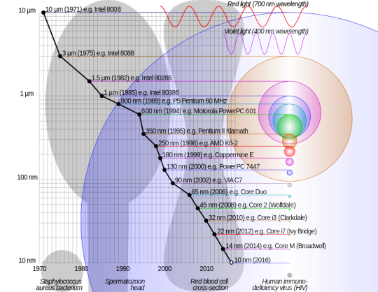
The Image above shows how tiny 14 nm really is. That tiny dot; smaller than the wavelength of a virus or even violet light.
At some point though, the doomsayers will be right. Quantum tunneling is a real thing that will prevent use of transistors with sizes of a new nanometers. This has lead Intel and other chipmakers to start looking in other directions (or other dimensions)
Three-dimensional integrated circuits (3DIC) is a technology that builds up, rather than in 2D like traditional wafer manufacturing technologies. For example, putting two 14 nm process wafers on top of each other doubles the transistor planar density without deceasing transistor size. Boom. Moore’s Law’ed.
(There are also some cool other benefits to 3DIC tech, such as increasing speed by decreasing distance between average length between components, and increasing sensor size of a camera by putting all of the logic underneath the CCD)
Thermocompression bonding is a common method of bonding two wafers to make a 3DIC. But it requires high temperatures (the “thermo” part) and high pressures (the “compression” part) that can damage the delicate and tiny devices on the wafers. Particularly, the high temperature is the biggest concern, so researchers have made efforts to develop room-temperature bonding methods.
One promising direction is to coat metals on both wafers, then grow metal grains across the bonding surface. Metals are composed of micro- or nano-scale grains of well-ordered atoms. Grains are very strong, since the atoms within them are well-ordered and don’t want to separate. Growing a grain between one wafer and the other would make for a strong bond, but that has been difficult to do at room temperature (which is why pressing two piece of metal together doesn’t make them stick).
My thesis is largely about nanoscale material structure, particularly in wafer bonding, and more particularly in metal-metal bonding.
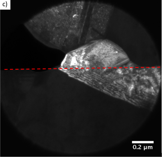
Above is a transmission electron microscopy image I took of a single grain of gold that has been grown across the bonding interface (shown in dotted red). The gold on one side is “nanotwinned”, which is really cool and something I’ll talk about soon.